
Printed Circuit Boards (PCBs) are the invisible backbone of modern electronics. Every time a smartphone connects to a network, a car’s control system responds to sensor data, or a medical device monitors vital signs, a PCB is operating quietly behind the scenes.
Although many people interact with devices daily, few fully understand how PCBs function or why they are so essential to modern engineering. This article explores PCB technology from foundational theory to manufacturing ecosystems, providing a structured and educational overview aligned with established engineering practices.
The Fundamental Purpose of a PCB
A PCB provides a structured framework that enables electronic components to connect and operate together in a controlled and predictable manner.
Before PCBs existed, electronic systems relied on point-to-point wiring. This approach was bulky, error-prone, and difficult to scale. The invention of the PCB revolutionized electronic manufacturing by replacing individual wires with patterned copper traces.
In practical terms, a PCB fulfills three main functions:
- Mechanical support for components
- Organized electrical signal routing
- Controlled thermal distribution
Without PCBs, compact computing devices, industrial automation systems, and advanced communication networks would not be feasible.
The Science Behind PCB Operation
Understanding PCB technology requires understanding the physical principles involved.
Electrical Conductivity
Copper traces act as pathways for electron flow. The width and thickness of these traces determine the amount of current they can safely carry without overheating.
The resistivity of copper is low, making it ideal for reliable current transmission. However, improper trace design can lead to voltage drops or thermal buildup.
Dielectric Materials
The substrate of a PCB is made from insulating material, typically FR-4 fiberglass epoxy. This dielectric layer prevents unintended electrical conduction between layers.
In high-frequency circuits, the dielectric constant of the substrate directly influences signal speed and attenuation. Engineers must carefully select materials to optimize performance.
Electromagnetic Behavior
High-speed digital signals behave more like waves than simple voltage transitions. As frequencies increase, trace geometry, spacing, and reference planes become critical for preventing reflection and interference.
This intersection of physics and engineering makes PCB design a multidisciplinary discipline.
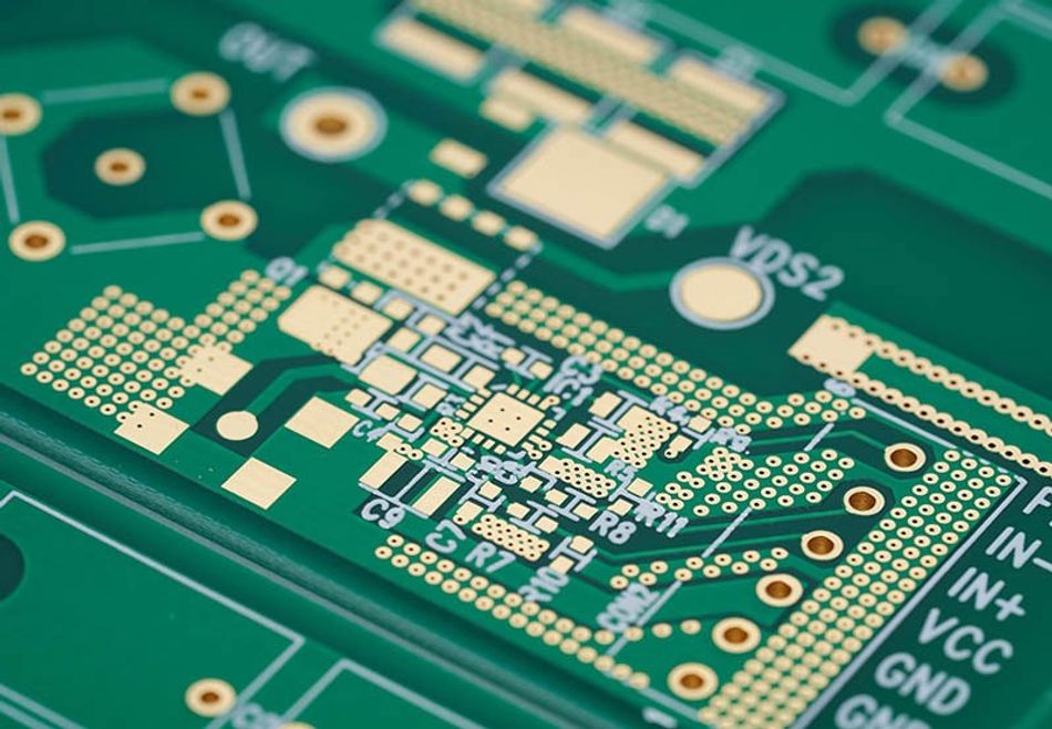
Anatomy of a Modern PCB
A PCB consists of layered components working together.
Substrate Layer
Provides mechanical rigidity and electrical insulation. For thermal-heavy applications, metal-core substrates may be used.
Copper Layers
Thin sheets of copper are laminated and etched to form circuit traces. Multi-layer boards may contain 4, 8, or more conductive layers.
Vias
Vias are plated holes that connect internal layers. Advanced boards use microvias to support dense, compact designs.
Solder Mask and Surface Finish
The solder mask protects copper traces from oxidation and short circuits. Surface finishes ensure reliable solderability during assembly.
PCB Design Principles
Effective PCB design is not simply drawing copper lines—it requires adherence to engineering rules.
Power Distribution Strategy
Power planes must minimize voltage drop and noise. Decoupling capacitors are positioned close to integrated circuits to stabilize voltage.
Signal Integrity Planning
Controlled impedance routing ensures high-speed signals maintain consistency across trace lengths.
Thermal Management
Engineers incorporate copper pours, thermal vias, and heat sinks to dissipate heat effectively.
Manufacturability Considerations
Designers must consider minimum trace width, drill tolerance, and layer registration accuracy to ensure cost-efficient production.
A strong understanding of global manufacturing ecosystems, including providers of china circuit board assembly services, can influence early design decisions and cost planning.
PCB Fabrication Process Overview
PCB production involves highly controlled industrial processes.
Imaging and Etching
Photosensitive layers define copper patterns. Chemical etching removes excess copper.
Drilling and Plating
Computer-controlled drilling machines create precise vias. Copper plating connects internal layers electrically.
Lamination
For multi-layer boards, layers are bonded together under heat and pressure to create a unified structure.
Quality Inspection
Inspection methods include:
- Automated Optical Inspection (AOI)
- X-ray inspection for inner layers
- Electrical continuity tests
Each stage ensures board integrity before assembly begins.
PCB Assembly Technologies
After fabrication, electronic components are mounted onto the board.
Surface Mount Technology (SMT)
SMT components are placed directly on the PCB surface and soldered via reflow ovens. This method enables high-density assembly and automated precision.
Through-Hole Technology (THT)
Components with leads are inserted into drilled holes and soldered manually or automatically. This technique provides strong mechanical bonds.
Manufacturers that specialize in china circuit board assembly services often combine advanced automation with scalable production capabilities to meet diverse global demands.
Reliability Testing and Industry Standards
High-quality PCB production follows internationally recognized standards.
IPC Standards
IPC guidelines define manufacturing tolerances, inspection methods, and acceptability criteria.
Environmental Testing
Boards may undergo temperature cycling, humidity testing, and vibration simulation.
Failure Analysis
Common PCB failure modes include:
- Solder fatigue
- Via cracking
- Delamination
- Electromigration
Preventing these failures requires careful material selection and design validation.
Industry Applications
PCBs are central to numerous sectors:
Consumer Electronics
Smartphones and wearable devices require high-density multi-layer boards.
Automotive Systems
Engine control modules and safety systems rely on vibration-resistant and heat-tolerant PCBs.
Medical Equipment
Medical devices demand high reliability and regulatory compliance.
Telecommunications
Routers and base stations depend on controlled impedance boards for signal integrity.
Industrial Automation
Factory equipment uses durable boards designed for harsh environments.
Each sector imposes unique performance requirements on PCB design and assembly.
Global Supply Chain and Manufacturing Ecosystem
PCB manufacturing is a global industry.
Design may occur in one country, fabrication in another, and assembly in a third location. China has emerged as a major hub for PCB fabrication and assembly due to scalable production capacity and technical infrastructure.
Global sourcing requires attention to:
- Certification standards
- Quality management systems
- Traceability and compliance
- Logistics and lead times
Collaboration between engineers and manufacturing partners improves time-to-market and cost efficiency.
Emerging Trends in PCB Engineering
PCB technology continues to evolve.
High-Density Interconnect (HDI)
Microvias and fine trace geometries support compact electronic products.
Flexible and Wearable Electronics
Flexible substrates enable curved and foldable devices.
Embedded Components
Passive components integrated into internal layers reduce footprint and increase reliability.
Smart Manufacturing
Artificial intelligence enhances automated inspection and defect detection.
Innovation in materials and design tools continues shaping the future of electronics.
Conclusion
Printed Circuit Boards form the foundation of modern electronic systems. They combine electrical theory, materials science, manufacturing engineering, and quality control into a single, integrated platform.
Understanding PCB fundamentals—from physics and materials to fabrication and global supply chains—provides valuable insight into the technology that powers today’s world.
As electronic devices become more compact, faster, and more complex, PCB innovation will remain at the center of technological advancement.